SPI (Serial Peripheral Interface)
SPI is a data communication protocol that we use for controlling devices within a subsystem, primarily sensors.
In this section, we will describe the SPI protocol and how to use our library with the ATmega32m1.
What is SPI?
SPI is a communication protocol used to communicate between microcontrollers and peripheral devices, such as sensors. Put simply, it’s a system that allows us to send a byte to some device and receive a byte in return.
SPI uses what’s called a Master-Slave architecture. In this system there is one master device that communicates to multiple slave devices. In our system the master device is our microcontroller and the slave devices are mostly sensors. The master can only communicate with one slave device at a time and the slaves cannot communicate with each other.
SPI Bus
SPI is a synchronous serial communication protocol used to communicate between devices. SPI uses a master-slave architecture, with a single master device initiating the communication frame, and operates in full-duplex mode (data is sent and received at the same time).
In digital systems, data is transferred in the form of 1’s and 0’s. In hardware, 1’s and 0’s are represented as high and low voltages. Our satellite uses 3.3V, so a 1 corresponds to ~3.3V on a wire, and a 0 corresponds to ~0V.
SPI is a synchronous communication protocol, meaning data is timed with clock pulses. is sent and received at the same time. This means that two of the four lines (MOSI, MISO) are for data, and one of the lines (SCK) is for timing.
SPI uses four wires to communicate, which are referred to as the SPI bus. Three lines (SCK, MOSI, MISO) are shared between all devices on a SPI bus. The fourth line (CS/SS) is unique to every slave device, and all CS/SS lines are connected to the master device.
The master device always transmits a square wave on SCK (source clock) to synchronize all devices. To initiate communication, the master device sets CS/SS (chip select/slave select) low for a particular device. The master device sends data to the slave device on the MOSI (master out, slave in) line. At the same time, the slave device sends data to the master device on the MISO (master in, slave out) line. To stop communication, the master devices sets CS/SS high again.
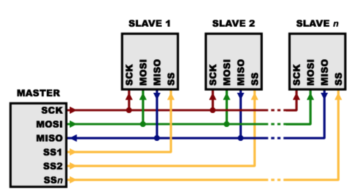 Diagram of a general SPI bus
SCK/SCLK (Source Clock)
The clock keeps the data lines and devices in sync. The clock is an oscillating signal produced by the master device that tells the receiving device when to read the data. Depending on the device properties, data is either sent/received on the rising/falling edge of SCK. We will discuss this in more detail shortly. This line is shared by all slave devices.
MOSI (Master Out Slave In)
This is the line where data is sent from the master device to the slave device. This line is shared by all slave devices.
MISO (Master In Slave Out)
On this line the data is being sent out of the slave device received by master. This line is shared by all slave devices.
CS/SS (Chip Select / Slave Select)
This line is referred to as CS or SS interchangeably. It is active low, which means the slave device is active when CS is set low. Only one CS can be low at a time or there will be conflicts on the SPI bus resulting in garbage data. We use a pull-up resistor on the CS pin to set a default value.
A pull-up resistor is a large resistor (typically 10K) which bridges between VCC (3V3 in our case) and another pin. When no load is applied to the pin, no current flows through the resistor. This allows us to hold CS at a known (3V3) state when the CS pin isn’t being driven by other circuitry. Then, we can drive another pin on the CS line low (GND) to select the device. Current will flow through the resistor and drop 3V3 across it.
Hardware Signal
If you look at the SPI lines on an oscilloscope, this is what a SPI transfer should look like:
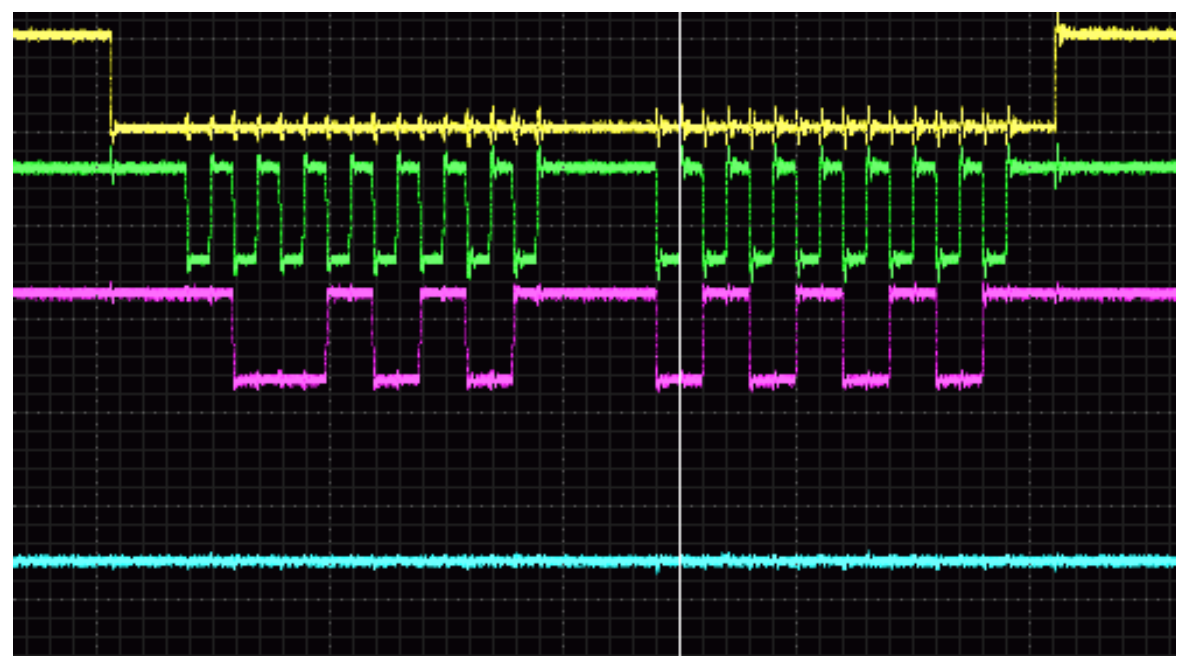 SPI signals on an oscilloscope
This image is taken from online but SPI transfers look very similar on our equipment.
I’ll pose the following question:
Which lines are which?
You can’t really distinguish between MISO and MOSI in this picture but just pick one to be MOSI and the other to be MISO. What is being sent and received? The answer is given below.
Answer:
- The yellow line is CS. This is because it is being lowered before and raised after the SPI transfer is complete.
- The green line is SCK. It oscillates 8 times for each byte sent.
- The pink and blue are MOSI and MISO. The blue line has
0x00and0x00and the pink line has0b10010101and0b01010101.
Using our SPI Library
Here are the basic software steps to send SPI messages.
Setup:
- Initialize SPI
- Initialize CS as an output pin
- Set CS high
Transmission:
- Set CS low
- Send SPI message
- Set CS high
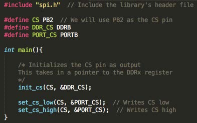
CS Pin
On our microcontroller each IO pin has three registers that control it. We will only need to use two of them. There is the data direction register that controls if the pin is input our output and there is the port register that lets you write high or low on the pin.
Once you figure out what pin you are using for CS you can check the microcontroller’s datasheet to get the name of the pin. Figure 1 shows the pin configuration for the ATmega32m1 microcontroller.
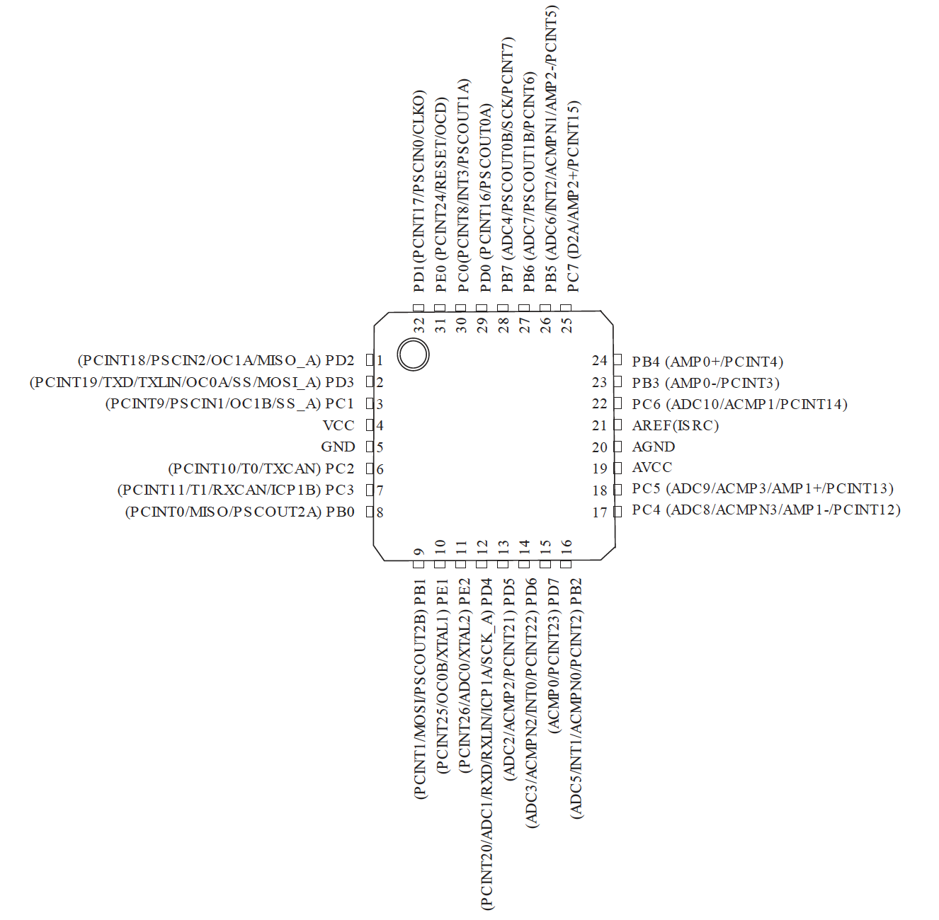 ATmega32m1 pinout
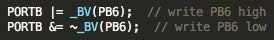
There are four banks of ports (B, C, D and E) with eight pins on each. There are 8-bit data direction and port registers for each of the four ports. Each bit in the register is for a separate pin. The data direction register is called DDRx and the port register is just called PORTx where x is the port. So if you wanted to initialized PB6 as output the code would be the following.
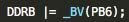
The macro _BV(PB6) expands to 1 << PB6 and PB6 is a macro that expands to 6. Here is the code to write high or low on PB6.
In our SPI library we have functions that will do this for you. This is how you use them.
Initialize SPI
We have a function, init_spi() that does this. It initializes SCK and MOSI as output and sets the SCK frequency to 8 MHz / 64. The 32M1’s internal clock frequency is 8 MHz.
Sending a SPI message
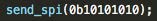
SPI sends 8 bit messages. If you want to send more than a byte you can send consecutive SPI messages. This is how you do it.
Example SPI Code
/*
Example from PAY:
Say we want to use the pin labelled PB5 on the 32M1 as the CS pin for the SPI device.
It uses pin 5 on DDR B (data direction register) and Port B (output).
*/

// This would be in a header file
#define CS PB5
#define CS_PORT PORTB
#define CS_DDR DDRB


// Setup: Just do this once

// Initialize SPI
init_spi();

// Initialize CS pin as an output pin
init_cs(CS, &CS_DDR);   // pin, DDR

// Set CS pin high (disable SPI device by default)
set_cs_high(CS, &CS_PORT);


// Transmission: do this every time you want to transmit

// Start transmission: set CS pin low (enable SPI device)
set_cs_low(CS, &CS_PORT);  // pin, port

// Send and/or receive data: call send_spi() for each byte
uint8_t received1 = send_spi(0xA4); // if you want to both send and receive
uint8_t received2 = send_spi(0x00); // if you just want to receive (send 0)
send_spi(0xA4);                     // if you just want to send (ignore received)

// End transmission: set CS pin high (disable SPI device)
set_cs_high(CS, &CS_PORT);
This is another full SPI program to make sure SPI is running correctly on the microcontroller.
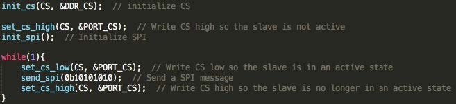
This repeatedly sends 10101010.
Clock Settings (advanced)
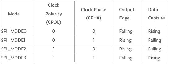
SPI has settings for the clock polarity (CPOL) and phase (CPHA), as described here. Usually the default settings work and you don’t need to worry about this, but occasionally there is a device where these settings must be modified. You can see what a device’s CPOL and CPHA settings should be based on the SPI timing diagram(s) in its datasheet.
The two clock settings introduced here are Clock Polarity and Clock Phase. Clock Phase determines whether data is shifted in and out on the rising or falling edge of the data clock cycle. Clock Polarity determines determines whether the clock is idle when high or low.